
Packaging Technology
Changes in Package Shapes of ICs and LSI devices
1980s
1980s: Era of QFPs for surface mountingMicrocontrollers and memory products became mainstream products replacing custom LSIs as the devices of the era in the 1980s. The demand for low-cost and portable electronic devices grew, and technologies for surface-mount packages were intensively pursued and established mainly in Japan. Standardization activities of the Electronic Industries Association of Japan (EIAJ) and the Semiconductor Equipment and Materials International (SEMI) advanced the standardization of package shapes, materials, and equipment.
1980: Development of FPGs with high heat-dissipation
A ceramic substrate with multilayered-wiring was used in developing the 160-pin FPG package for surface mounting. Good heat-dissipation characteristics were achieved by attaching aluminum heat-dissipation fins after mounting of the package on the printed-circuit board. This package was used in mainframe computers in which the LSI circuits are cooled by an air-cooling system.
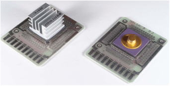
Examples of High Heat Dissipation FPG
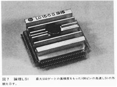
High Speed Logic LSI in High Heat Dissipation Package
1982: Development of MSPs
The MSP (mini square package) was developed as a compact package to incorporate analog ICs etc. for surface mounting in camcorders for consumer use. This package allowed near-vertical mounting of the lead pins on the printed-circuit board, miniaturizing the footprint and thus contributing to further reductions in the sizes of camcorders.
MSPs (Mini Square Packages)
1982: Applying chip-on-board (COB) technique to LSI circuits
In the chip-on-board technique, the areas for mounting LSI components on printed-circuit boards are hollowed out by the router and the LSI devices are embedded in these areas. This enabled the further development of such small electronic devices as digital watches, telephone cards, and thermometers. This also cleared the path to the application of resin substrates to LSI circuits.
COB Technologies
1985: Establishment of technology for surface mounting
Despite the development of various surface-mount packages, methods for soldering devices to printed-circuit boards had not been consolidated. For this reason, the Semiconductor Device Package Committee of the Electronic Industries Association of Japan (EIAJ) played a central role in running educational campaigns to promote the development of soldering methods, materials, and equipment, further establishing surface-mounting technology (SMT).
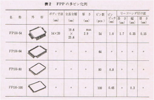
Increasing Nimber of Pins in FPP
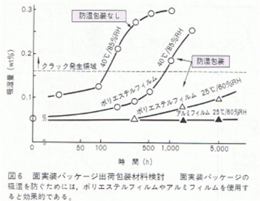
Study of Shipping Package Material for Surface Mount Packages
1985: Development of ultrasonic inspection technology
Development of the reflow soldering method for printed-circuit boards accompanied the continued increases in the mass production of surface-mount packages. However, this led to more cracks in the resin forming the packages and to breaks in gold wiring, so ultrasonic inspection was developed to check the adhesiveness of LSI devices and lead frames for these problems.
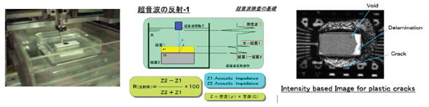
Ultrasonic Inspection Technology
1986: Introduction of ion chromatography testing
The reliability testing of resin-mold packages had revealed failures due to aluminum around bonds becoming corroded to be the biggest problem. Examination showed that fillers added to the resin material, components such as lead frames, and impure ions mixed in during production were the reasons, so processing to control impure ions was introduced. Introducing this method of testing improved the reliability and quality of resin-mold packages, which then came to be adopted for use in such LSI devices as microcontrollers and memory products.
Ion Chromatography Analysis of Contaminating Ions
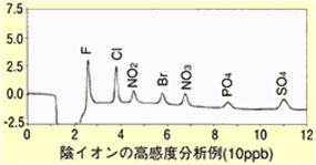
Example of High Sensitivity Analysis of Negative-Ions
1986: Reporting QFP design outline to the world
In order to make QFP that was developed in Japan become a global standard, the Electronic Industries Association of Japan (EIAJ) presented the design concept and advantages of the QFP at an international conference on semiconductor packages called the IMC (International Microelectronics Conference). This was the first introduction of the QFP to overseas as a package with large numbers of pins.
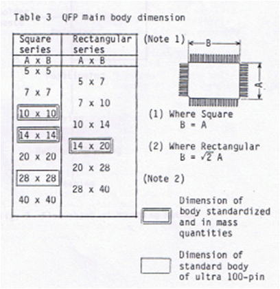
QFP Main Body Dimentions
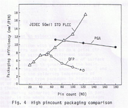
High Pin Count Packaging Comparison
1986: U.S. files for an injunction against the import of DRAMs in PLCC-type packages
Feeling threatened by Japanese and South Korean possession of the DRAM market, the U.S. filed a suit at the International Trade Commission requesting an injunction to prohibit the import of DRAMs manufactured by nine Japanese and South Korean companies on the grounds of the unauthorized use of a DRAM patent held by Texas Instruments Inc. In response to this, the respective companies argued that standardization committees such as JEDEC had discussed the plastic leaded chip carrier (PLCC) structure, pointed out differences in the method of manufacturing, and raised other points. The production of 64-Kbit DRAMs continued following the settlement of the dispute.

Cross Section of PLCC Package after Mounting
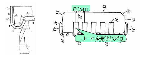
1987: Establishing a method for mounting TAB packages in LCD TVs
Matsushita Electric Industrial Co., Ltd. adopted the TAB method in a 10-inch color liquid crystal display (LCD) TV set. An anisotropically conductive film formed by scattering fine metal powder in resin was used to connect the TAB-type LSI to a transparent indium–tin oxide (ITO) film which formed the LCD panel electrodes.
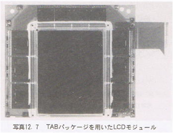
LCD Module with TAB Packaging
1988: The first Japan&U.S. Semiconductor Package Joint Committee in Hawaii
In order to spread packaging techniques being developed in Japan, such as the QFP, the Electronic Industries Association of Japan (EIAJ) intensified standardization activities around 1985, and held the first Japan-U.S. Semiconductor Package Joint Committee in Hawaii. Japan made proposals on methods for the naming of packages and the notation for package dimensions, and urged the use of the millimeter as the standard unit. After convincing the department in charge of military specifications and standards among others, the U.S. accepted the change from the inch to the mm as the standard unit of measurement in package design. The STS (SEMI Technology Symposium) session was set up within the same year at SEMICON Japan, hosted by SEMI Japan, to provide an opportunity to present packaging techniques.
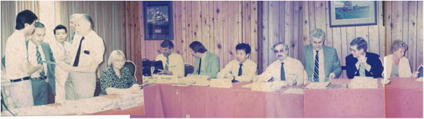
First Japan-U.S. Semiconductor Package Joint Committee (@ Hotel in Hawaii)
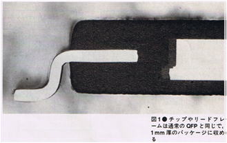
1988: One-mm-thickness QFPs enter mass production
Hitachi developed the thin TQFP (thin quad flat package), a resin package with a thickness of only 1.0 mm. Following its introduction, the package came to be used for memory devices such as DRAM and SRAM as a measure towards even smaller and lighter electronic devices.
Cross Section of TQFP (1mm Thickness)
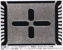
Countermeasure to Cracks by Cross-Shape Slit in Die-Pad
1988: Start of LOC structure development
As a technique for the high-density mounting of DRAM, Hitachi also developed the lead-on-chip (LOC) structure, in which the lead frame is placed above the DRAM chip and connected with gold wiring. This structure led to the SOJ (small-outline J-leaded) package and pin-insertion ZIP (zigzag in-line package).
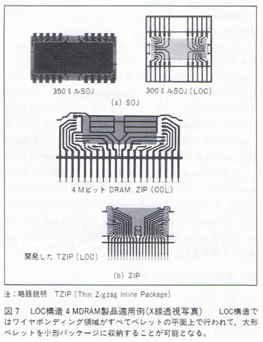
4Mbit DRAM with LOC Type Package - X-Ray Photo
1989: Development of 208-pin QFP packages with two internal lead-frame (LF) layers
As the operating frequencies and numbers of pins of LSI devices continued to increase, the noise from signals in the lead frame became a problem. Hitachi thus developed a 208-pin QFP package with a two-layer structure in which a ground layer was formed beneath the lead frame. This package was applied to LSI circuits for mainframe computers among other products.

QFP Package for High Speed Device with Two Internal Lead-frame Layers