
Process Technology
1990s
In the 1990s, due to the advancement of miniaturization of processes, the enlarged scale of production, and larger wafer diameters, huge investment scale like several hundred million dollars per factory initiated “investment race.”
Owners of mega-fabs and equipment manufacturers proceeded towards oligopoly. In addition, South Korea and Taiwan started to catch up, and the outflow of process technology associated with the flow of domestically produced equipment at the world-class level to foreign countries was said to be a contributor to decline of competitiveness of Japanese semiconductor industry.
Early 1990s: Transition to 200-mm (8-inch) wafers
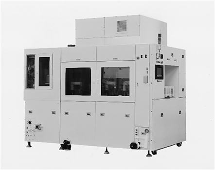
Wafer diameters were successively increased to improve manufacturing efficiency, and manufacturing lines switched to the use of 200-mm wafers in early 1990s.
The entire industry was faced by a decline in yield ratios due to strain caused by heat stress, and the vertical furnace was developed as the countermeasure.
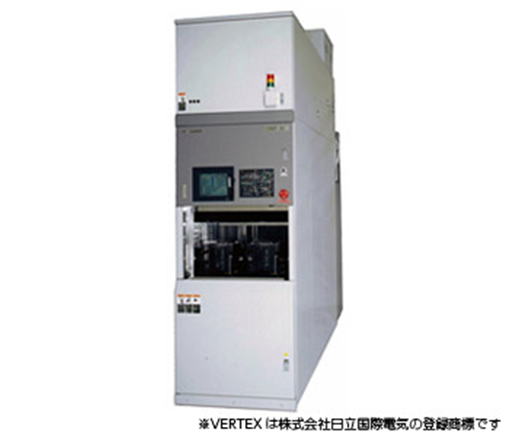
Vertical diffusion furnace
Early 1990s: High-density plasma (ECR: electron–cyclotron resonance and ICP: inductively coupled plasmas) etching and CVD
In order to embed silicon dioxide in microtrenches and to etch deep holes, high-density plasma (HDP) equipment was developed and started to be used in production. Equipment manufacturers such as the Canon Anelva Corporation, Hitachi, the Lam Research Corporation, Novellus Systems, Inc., and Applied Materials, Inc. started production one after another.
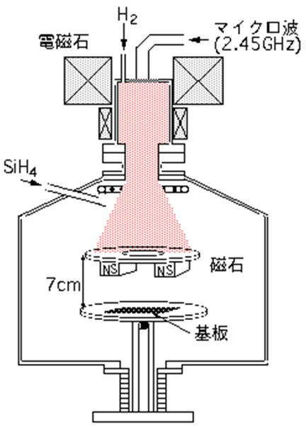
Schematic of ECR (Electron-Cyclotron Resonance)-CVD
Around 1990: Usage of shallow junction and silicide source/drain techniques
As junctions became shallower with advancing miniaturization, measures to realize the conflicting requirement of lowering resistance were needed.
When ion implantation is used to make a very shallow junction, the resistance becomes greater. To get around this, a silicide technique where a silicon–metal alloy is deposited on top of the diffusion layer was adopted.
1990s: Start of mass production of single-wafer equipment
As plasma methods came to be widely used in etching and CVD, single-wafer equipment for the processing of one wafer at a time became the mainstream. Similarly, annealing equipment and cleaning equipment were appearing in single-wafer forms. The advantage was greater accuracy in wafer processing.
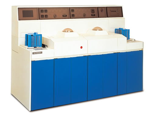
Single-Wafer Cleaning Equipment of SPW Series
Late 1990s: Shorter wavelengths of exposing sources (from the i-line of mercury emission to excimer laser beams)
As miniaturization continued to advance, raising the resolutions of exposing equipment became essential. Accordingly, the numerical apertures (NAs) of lenses were increased and steppers with exposing sources having shorter wavelengths came into use. In the early 1990s, the i-line from a mercury lamp provided the source of light. By the late 1990s, krypton-fluoride excimer laser beams were being used. As a result, an LSI with minimum feature dimensions of 250 nm was achieved.
Late 1990s: Usage of chemical–mechanical polishing
Chemical–mechanical polishing (CMP) began to be used as a technique for obtaining extremely flat surfaces in the late 1990s. One advantage of the CMP technique was that flattening enabled miniaturization by allowing the decreases in depth of focus in lithography.
CMP equipment of the dry-in/dry-out type was developed in Japan, allowing the installation of CMP equipment in clean rooms. This contributed to the practical application of CMP equipment.
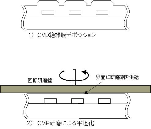
Flattering Process by CMP
Early Dry-In/Dry-Out CMP Equipment
Late 1990s: Adoption of shallow trench isolation (STI)
When miniaturization further advanced to see in the 0.35-m generation, STI came into use for element isolation. The HDP-CVD technique for embedding insulators in microtrenches and the CMP technique for flattening surfaces both contributed to the implementation of STIs.
Late 1990s: Adoption of the damascene method to form copper interconnect.
Aluminum was replaced by copper to reduce wiring resistances. However, since there was no suitable method for the etching of copper, the damascene method was used to fabricate copper interconnect. CMP is an essential part of the damascene method.