Japan Semiconductor Innovation 50 (T-1 1960s)
De-facto Standardization of <100> Crystal Orientation for MOS Devices (Hitachi)
Ohno, et al. of Hitachi invented a method of "heat
treatment with electrical bias" on MOS structures in 1963, which enabled
the control of mobile ions in the oxide films. Kerr of IBM reported a similar
result as "B-T Treatment" or bias-temperature treatment next year,
and this naming has been widely used, since.
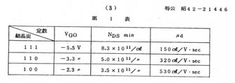
As the result of further research by using this method, Ohno and his team
proved that using the silicon <100> plane as the channel was most
advantageous for MOSFETs, because it minimized the fixed charges and surface
states at the interface between the silicon substrate and the oxide film.
The silicon wafers with <100> surface orientation have been used for
most MOS LSI circuits as de-facto standard substrate. Their invention played
substantial role in realizing the practically useful MOS devices.
Characteristic comparisons of MOSFET published in Japan patent specification |
 |
| From Japan patent bulletin |