7) A Tokyo Univ. Group’s “Solid-State Logic Circuit”

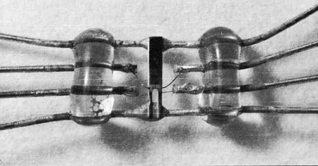
Picture A: One of the first ICs developed by a collaborative effort between
Tokyo University and NEC

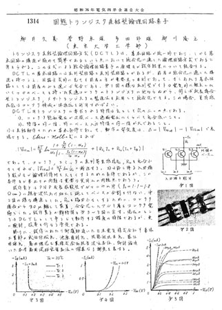
Picture B: Thesis presented at the Joint Convention of the Four Electrical
Engineering Institutes in 1961
(click to enlarge)
If we were to go on the subject of where Japan’s true first
“Monolithic IC” was made, the chip developed by a group of the University
of Tokyo in the collaborative research and development work with NEC would
be one possibility.
This is shown in the 4th Joint Convention Record of the Four Electrical Engineering
Institutes, held in 1961. In the thesis titled, “Solid-State Transistor Direct-Coupled
Logic Circuit Components” four members of engineering department in the University
of Tokyo at the time - Hisayoshi Yanai, Takuo Sugano, Kunio Tada, and Takashi
Yanagawa were included. At the convention held on April 8th, 1961, this was
presented together with the previously mentioned work (Ref. “Electricians
Inspired by an Magazine”) by Electrotechnical Laboratory group – later Research
Institute for Electrical Communication (RIEC). The work by RIEC was already
published in a newspaper at the end of January, and it was earlier by several
months in that sense. By the way at the end of February, Mitsubishi Electric,
following the technologies used at Westinghouse Electric, created 11 types
of “Molectron” products.
The “solid state” in the title was expressed using Chinese characters or kanji,
meaning more like “solid form,” which is somewhat odd, and it was changed
to today’s ordinary “solid state” in the second report.
As shown in picture A, this IC consists of two bipolar transistors (grown
junction type) and one negative resistance integrated on a germanium substrate
with a total length of about 5 mm, and the circuitry was Direct-Coupled Transistor
Logic (DCTL) NOR gate.
With transistors in the lower half and negative resistance in the upper half,
two transistors were separated from one transistor of which each part of the
emitter, base and collector had a slit made by ultrasonic processing.
Picture B is of the thesis presented at the Joint convention held in 1961
(Provided by Kunio Tada)
| To page top | To Part 2 index |