Japan Semiconductor Innovation 50 (D-1 1950s)
Invention of tunnel diode - Esaki diode (Sony)
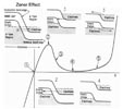
In 1957, Leo Esaki of Sony (then Tokyo Tsusin Kogyo -Tokyo
Communication Iindustry) discovered a negative resistance characteristics
in the current-voltage characteristics of very highly doped PN junction,
and he demonstrated that it was a tunnel phenomenon predicted by quantum
theory.
This result was reported at the fall conference of the Physical Society
of Japan in the same year and also at the international conference in Brussels
next year. This report was highly valued by Shockley, who was the inventor
of transistor.
In 1973, the Nobel Prize for Physics was granted to this accomplishment.
Since the negative resistance characteristics can be applied to high frequency
oscillation, amplification, fast switching, etc., the diodes using various
materials, such as germanium, Si, and InSb, were developed, and they were
called "Esaki diodes" or "tunnel diodes".
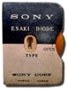
Esaki diode in shipping pakcage |
I-V characteristic of Esaki diode | Dr. Reo Esaki |
 |
 |
 |
| Offered by Dr.Esaki | Quote from ENCORE | Offered by Sony |
Remarks