Japan Semiconductor Innovation 50 (T-5 1970s)
Ultra-Thin Oxide-Nitride Gate Insulator Films (Fujitsu)
Fujitsu demonstrated that silicon-oxide-nitride films, formed
by thermal treatment of oxide films in activated nitrogen gas, were superior
to silicon thermal oxide films as the gate insulator of MOSFET, first in
the world in the latter half of 1970's.
These films were not practically used in this timeframe, but early adoption
started in the 90nm generation in which the gate insulator of 2nm and below
was used, and it became a standard technology in the 65nm generation. Adoption
of High-k films started after the 45nm generation, but the oxide-nitride
barrier layer on the silicon interface is regarded to be indispensable.
This technology, in which Japan took the initiative, became essential one
in high-performance CMOS LSIs in the global semiconductor industry, and
will most probably be used in the future generations, too.
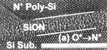
A part of 90nm CMOS TEM photo |
 |
| Reference 1 |
Remarks
Photo reference 1
"Electrical properties of 1.5-nm SiON gate-dielectric using radical
oxygen and radical nitrogen" IEEE Trans. ED, vol. 49, pp. 1903-1909
(2002)