Japan Semiconductor Innovation 50 (T-11 1980s)
LOC Type Package (Hitachi)
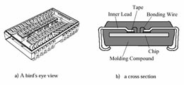
As the DRAM densities and die sizes increased, mounting of large dies in small outline packages became an important issue. Hitachi invented an LOC (Lead-on-chip) structure which minimized the difference between die size and package size. In this new structure, the chip layout was changed in such a way that bonding pads were located in the center of chips instead of conventional chip peripheral layout, and the package lead frames were positioned over the chips. Hitachi started the development of this technology in 1988, and jointly developed and commercialized 16MDRAM in the LOC package with TI in 1991, who was then the joint development partner of DRAM. High reliability and high density assembly was realized, and electrical characteristics were improved at the same time. This package type was later adopted widely as the industry-wise package technology.
Structure of LOC package |
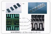
LOC package and 64M DRAM |
 |
 |
| Quote from main gallary of shmj | |
Remarks
To
main gallery (Packaging Technology 1980s)
- 1988: Start of LOC structure development
To
main gallery (Packaging Technology 1990s)
- See 1991: Announcement of the adoption of an LOC structure for 16-Mbyte
DRAM