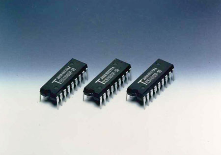
14) Toshiba’s Victory in Breaking “1M bit DRAM Wall”

Toshiba’s 1M bit DRAM (Provided by Toshiba)
Japanese DRAM manufacturers lagged behind US manufactures
in the initial three generations up to 16K bit. But in the 64K and 256K bit
generations, they dominated the market, and stood ahead of oversea manufacturers.
But even for Japanese manufacturers, the 1M bit DRAM wall was very high.
Initially, Fujitsu took a lead in the race. Fujitsu used the same NMOS structure
as before, but as for the memory cells, they adopted the trench structure
invented by Hitachi to which Fujitsu implemented improvements to realize the
cell size of 27μm2, 1/3 of the previous 256K generation.
Against this, Toshiba, who was somewhat lagging behind in DRAM market, took
the third way combining the planar cell structure with low power CMOS technology.
Other DRAM manufacturers were surprised at Toshiba’s approach of adopting
CMOS technology in the midst of mainstream NMOS technology. Tsuyoshi Kawanishi,
Toshiba’s General Manger of Semiconductor Division at that time, (later Toshiba’s
Senior Executive Vice President, and former SSIS Chairman) looked back and
commented, “We believed the low power CMOS would be the main stream in megabit
era, and we just moved in this direction”. Actually, Toshiba reduced the operation
power into 150 mW, which was less than half of NMOS. He also added, “We thought
the planar cell structure would be better suited for mass production than
three dimensional trench structure. This structure had merit to utilize the
conventional 256K DRAM manufacturing equipments.”
As a result, Toshiba established monthly capacity of one million pieces in
1986, and took a lead in this market. (The picture is Toshiba’s 1M bit DRAM,
provided by Toshiba)
Speaking of megabit chips, I appeared in the TV program called “Business Network”
in NHK Education TV as a commentator in February 1985, and I commented on
the VTR titled “Megabit was developed in this way” filmed at Hitachi’s development
site and others. The leader in this development team at that time was Tsugio
Makimoto, current SSIS Chairman.
| To page top | To Part 2 index |