31) The LSI Joint Research Laboratory and the Power of Cooperation

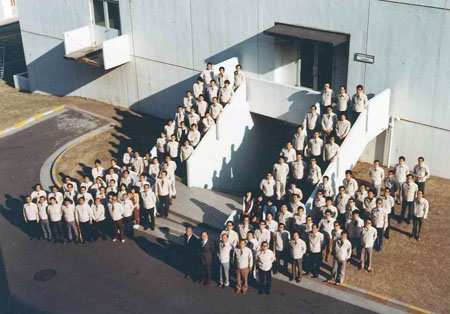
All of the members gathered at the entrance of the VLSI Joint Research Laboratory
The VLSI Joint Research Laboratory became the literal center of the VLSI project.
Researchers from the five participating companies and the Electro Technical
Laboratory (ETL, now the National Institute of Advanced Industrial Science
and Technology (AIST)) were dispatched to the research institute, and worked
on the research of VLSI as a next generation semiconductor technology. As
a result, this project was highly successful and was highly appreciated both
domestically and abroad, but it developed into a big controversy in trade
tensions between Japan and the US as a specific industry development policy
(“targeting”) by the Japanese government.
In the story told by Yasuo Tarui, who was appointed to be the Institute Director
by ETL, one of the success factors was that "the focus of choosing research
theme was on the fundamental and common problems". For this reason, it
was narrowed down to basic technologies such as microfabrication technology
and crystal technology, and design techniques close to product technology
were omitted.
The other success factor was to focus on creating an environment with team
atmosphere of ”cooperation is virtue”, which is actually very Japanese way.
With as many as 100 researchers gathered together from five different companies,
100 different opinions may lead to no conclusion, but on the contrary, if
researchers with these unique ideas can successfully work together, something
new will come out. Although the researchers were on a leased facility from
NEC Central Research Laboratory, the full time work of all the researchers
in one facility gradually cultivated “alumni mentality from eating from the
same rice cooker” (by Tarui) and “the benefits of cooperation” were clearly
seen.
Photo: All the members gathered at the entrance of the collaborative laboratory.
(Provided by Mr. Yasuo Tarui)
| To page top | To Part 2 index |