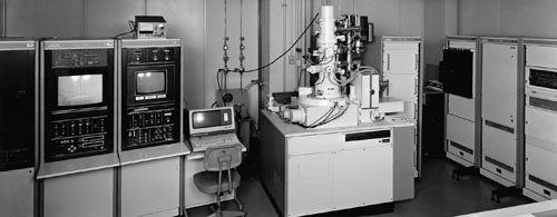
32) Impressive Achievements in Microfabrication Equipment

High-speed electron beam lithography equipment by variable dimension shaping
method
At the VLSI Technology Research Association, one of the development themes
was the promotion of research and development of manufacturing equipment such
as exposure equipment as a part of microfabrication technology, and the picture
above is of high-speed electron beam lithography equipment by variable dimension
shaping method. In conjunction with another equipment by field emission electron
gun type developed concurrently, it showed its power in mask making thereafter.
In 1967, Yasuo Tarui, the head of the research association had developed an
electron beam exposure apparatus in collaboration with Nihon-Denshi (JEOL
Ltd.) in his former position at ElectroTechnical Laboratory. He also succeeded
in creating a prototype MOS type transistor (channel length 1 μm) in 1969.
These achievements helped the development of high-speed electron beam lithography
equipment at the research association.
Another achievement was a reduction projection exposure apparatus, later to
be called a “stepper”. At that time, ultraviolet exposure was a single step
one-to-one projection to the whole wafer, but the issues such as resolution
and dust, in addition to larger wafer diameter and miniaturization of processing
dimensions, became the problems to be solved. Therefore, the method of reducing
numbers of chips in a reticle to one and exposing one chip pattern at a time
with repetition was developed.
Shoichiro Yoshida (later to be the President of Nikon and former Vice Chairman
of SSIS) who was in charge of prototyping this equipment said, "We have
long wanted to do a step-and-repeater with a positioning mechanism by interferometer
and high-resolution lens.
So, we were very enthusiastic about the product development, and we made a
lot of efforts. The fact that we are doing well in the world market today
is a gift from this."
| To page top | To Part 2 index |