33) Japan’s Original Technology – Flash Memory

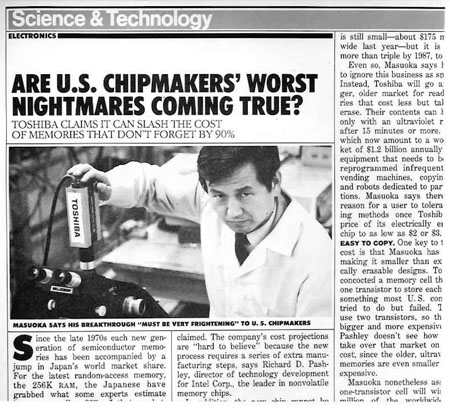
The article from “Businessweek” magazine, reporting on the development and
result of flash memory
(click to enlarge)
With its peak in the 1980s, Japan enjoyed the name of "memory powerhouse"
and it’s "special product", flash memory. Fujio Masuoka, who was
employed at the Toshiba ULSI Research Laboratories (later a professor at Tohoku
University) succeeded in its development in 1980 and first presented his work
at the International Electronic Devices Meeting (IEDM) in December 1984.
The origin of the name “flash” came from consulting with his colleagues, seeking
for some catchy name to the audience of IEDM. The concept of collective or
batch erasure was superimposed on an image of a flash of light.
The photograph is an article from the magazine “Businessweek” which conveys
his accomplishment, but while highly appreciating Masuoka's creative achievement,
it also included opinions of persons at Intel saying, "The manufacturing
process is too complicated and not feasible". Seeing that Intel later
created their own flash memory division and actively promoted this business,
it is highly ironic.
At the time of development, Masuoka told me that "This type of memory
will become the driving force of the semiconductor industry in the beginning
of the 21st century." But if we look at the fact that it is shaking up
the position of the hard disk as an information storage medium, his dream
was a genuine “prophetic dream”.
| To page top | To Part 2 index |