2) A Nobel Prize Born from a Failure Analysis

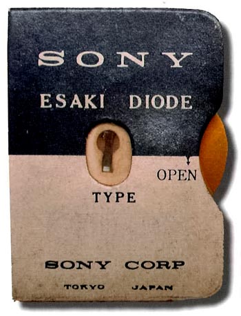
Sony's Esaki Diode
Leo Esaki won the Nobel Prize in Physics for the tunnel diode
(Esaki diode), which was actually born from the failure analysis of a transistor
for radio application.
In the mid 1950's, Sony developed a transistor with an increased concentration
of impurities (phosphorus) in germanium crystals, but faced the problem of
large quantities of defective products. The higher the impurity concentration,
the higher the amplification factor of the device. How far can you increase
the impurity concentration without destroying the properties of the crystal?
Esaki, who was just transferred from Kobe Industries, was appointed to do
this task.
"It was a hot day in July 1957," he recalls. While investigating
the PN junction diode in a bath at -80°C, we discovered "negative resistance"
which is that the current flow decreases as the voltage applied increases.
This very phenomenon is a tunneling effect predicted by quantum mechanics,
and it was a sign that would lead to the birth of the Esaki diode. He thought
that this phenomenon could be used to create a high speed device capable of
switching and amplifying currents.
Esaki presented his findings at the conference of the Physical Society of
Japan in October 1957, but it did not attract much attention. It was at the
1958 International Solid State Physics Conference held in Brussels where it
really got attention. W. Shockley, inventor of the transistor, mentioned the
result and Esaki in his keynote. As a result, Esaki's lecture was packed over
expectancy, and with that, researchers from all over the world had acknowledged
his presence in the field.
The photo is of a Sony Esaki diode. (Provided by Leo Esaki)