6) The Birth Place of "Super Lattice"


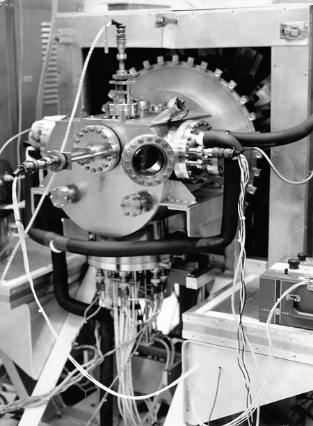
Picture A (left): Molecular beam epitaxy apparatus
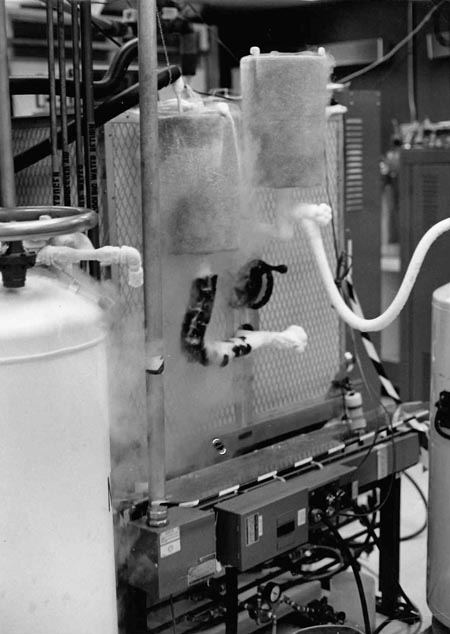
Picture B (right): Backside of the apparatus. Cooling the molecular beam generation room by liquid nitrogen.

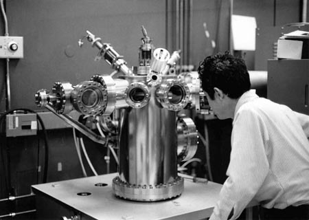
Picture C: Esaki studying the crystal growth mechanism using the Auger electron spectroscope (resolution 10Å)
Esaki, when moved to IBM T. J. Watson Research Center in 1960,
felt that he wanted, by being away from Esaki diode research work, to do a
large scale research work only possible in USA. This thought led him to his
proposal of a unique concept of “Super Lattice” in 1970.
In May 1974, just after Esaki’s Nobel Prize winning, I visited him at Watson
Research Center, and looked around the super lattice laboratory thoroughly.
The highlight was molecular beam epitaxy apparatus developed by the laboratory
to create the semiconductor super lattice. This apparatus, by spraying beams
of thin film forming materials like Gallium molecules onto the substrate in
high vacuum, realizes epitaxial growth of crystals with the aligned plane
with the substrate.
The beauty of this apparatus is to control the film thickness precisely in
nanometer order, by computer control of shutter on/off of molecular beam.
In Japan, at that time, this kind of apparatus was not available at all, and
people only obtained the information through academic conference presentations.
Picture A is molecular beam epitaxy apparatus controlled by computer. This
was called system A.
Picture B is the backside of the apparatus, cooling the molecular beam generation
room by liquid nitrogen.
Picture C is Esaki studying the crystal growth mechanism using the Auger electron
spectroscope (resolution 10Å). This apparatus was called system B together
with SHEED, ion sputtering gun and so on.