9) Ingenious Idea of HEMT

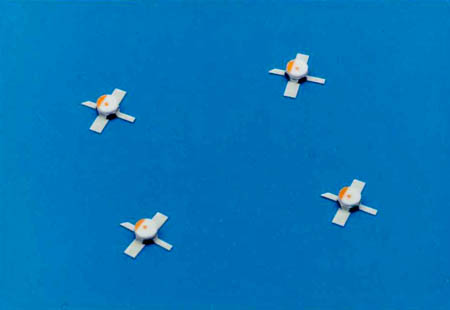
Picture: HEMT used in satellite broadcasting receiving converter
The world first device to make Esaki proposed Super Lattice
for practical application is high electron mobility transistor (HEMT). Takashi
Mimura, Fujitsu Laboratory's Senior Researcher (currently Fellow) developed
it in 1979.
Mimura's remarkable idea was that he picked up only one pair from the tens
to nearly hundred layers of super lattice structure and made it into transistor.
In the two layer structure, the second layer, electron supply layer, is aluminum-gallium-arsenic
layer and the first layer, electron transit layer, is less impurities gallium
arsenide layer. Electron move from the second layer to the first layer is
caused by the difference of electron affinity. When electron goes down to
the first layer, it moves at ultrahigh speed like the car drives at full speed
in the highway. As a result, operating speed improves and high frequency signal
reception and amplification becomes possible. As you know, at present, HEMT
becomes an indispensable device for like, converter of satellite broadcast
receiving antenna and car navigation system and mobile phone using GPS.
Mimura, who was in mid-thirties young researcher with full of energy when
he developed the device, explained me with humor in the interview that "In
short, it is like to relieve from parent's restraint, and to raise the original
ability". It was very impressive to me.