10) The Pioneer of Quantum Devices

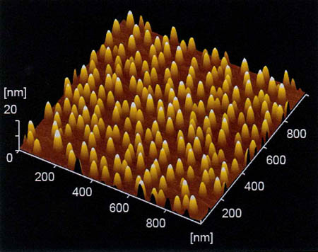
Picture A: An Atomic Force Microscope (AFM) image of indium arsenide quantum
dots
self-formed on a gallium arsenide substrate

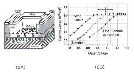
Picture B: the structure (A) and I-V characteristics example (B) of the photodetector

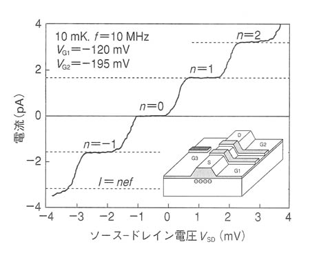
Picture C: A schematic structure of the element capable
of controlling the transport of a single electron made
by a fine lithography and V-I characteristics example
Hiroyuki Sakaki, also known as "Sakaki of Quantum Devices" drew attention from all over the world. It is an interesting story in how he got involved in this research.
Sasaki graduated from the Faculty of Engineering at the University of Tokyo in 1968, but the department he learned was Electrical Engineering Department, which was only slightly related to "electronics", and he thought that he would like to do jobs related to power generation in the future. He turned out to be a semiconductor researcher because he felt sensitive about the flow of the times, and after graduation began work on MOS type FET, based at Institute of Industrial Science, the University of Tokyo.
Sakaki was enlightened by quantum engineering because he was surprised upon reading Esaki's superlattice paper. Sakaki thought that it might be linked with his past research, and he devised basic concepts of "quantum wire" and "quantum dot" as a method of controlling the transport of electrons in thin films in 1975.
In the approaches to the same superlattice, Esaki drew negative
resistance characteristics by flowing a current in the vertical direction,
while Sakaki was interested in increasing the electron mobility in the thin
film by passing a current parallel to the surface.
He had worked for two years from 1967 at IBM Thomas J. Watson Research Center
by Esaki’s invitation, which later turned out to be very beneficial in the
validation of this hypothesis.
Currently, Sakaki is the president of Toyota Technological Institute and has
a hobby of painting appreciation, and says, "I am fascinated by the paintings
which have painter’s personal styles." Given that Sakaki's research is being
applied to the development of photodetectors and solar cells as well as semiconductor
lasers, and furthermore to the study of single electron transistors and quantum
computers, we can see that the spirit of making use of "individuality" is
also dynamic in his research activities.
Figure A is an Atomic Force Microscope (AFM) image of indium arsenide quantum dots (nano-particles) self-assembled on a gallium arsenide substrate. Embedding nanoparticles similar to this figure in the luminescent layer of laser, the quantum dot laser proposed by Yasuhiko Arakawa and Sakaki in 1982 has been realized.
Figure B shows the structure (A) and the V-I characteristics example (B) of the photodetector, in which the self-assembled quantum dots are buried near the surface of the conductive channel layer of the gallium arsenide FET. In the latter case, if electrons or holes are captured in the dots, it can be seen that the V-I curve is shifted from side by side.
Fig. C is a schematic figure of the structure of the elements capable of controlling the transport of a single electron made by a fine lithography and V-I characteristics example. In an element in which two gates for controlling the transport of single electron and a micro-space capable of storing a single electron are provided in a narrow wire channel, the phenomena of single electrons passing through one by one appears.
(Provided by Hiroyuki Sakaki)