15) A Research Life Fascinated by Blue Light Patent

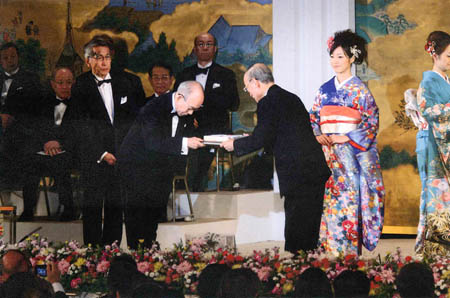
Picture: Akasaki receiving the Kyoto Prize in 2009 ( by courtesy of the Inamori
Foundation)
In light of the "blue era" in which Picasso expressed human
suffering in blue, light emitting diodes (LEDs) are also in the middle of
it.
It was Isamu Akasaki who is a professor at Meijo University and also a special
professor at Nagoya University who first opened the door leading the way to
blue LED era.
Among researchers, gallium nitride, which has a large band gap, had been known
as a promising material for blue light emission, but it is difficult to produce
crystals because of its high melting point similar to diamond, and eventually
zinc selenide had become the primary candidate material. Under such circumstances,
Akasaki thought that if epitaxial film growth technology was applied effectively,
it would be possible to produce high-quality gallium nitride thin film without
cracks and irregularities.
In May 1981, he made a prototype blue LED with a luminous efficiency of 0.12%
and luminous intensity of 2 mil candela using the MIS structure.
Akasaki thought that it was far from practical use, and as a next step, he
formed a buffer layer of aluminum nitride on the sapphire substrate, and then
grew a high-quality gallium nitride film on it. As a result, the mismatch
of the thermal expansion coefficient between sapphire and gallium nitride
was eliminated, and a foothold for high luminance emission was achieved. It
was in 1985. Hiroshi Amano (currently a professor at the University of Tokyo)
who was a graduate student at the time contributed to the idea of this method,
and the patent in Japan and the United States was obtained.
Furthermore, the formation of a PN junction type device was also achieved
by a breakthrough technology which is to irradiate magnesium-doped gallium
nitride with electron beams.
The photo is of Akasaki who won the 2009 Kyoto Prize. "It was a research life
fascinated by blue light from the beginning of my 40s," he said. In 2011,
he was honored with the Order of Culture following the award of the Edison
Award, and he was awarded Nobel Prize in 2014.