
Discrete Semiconductor Devices, etc.
1970s
1970: Success in continuous-wave (CW) operation of a semiconductor laser diode (LD) at room temperature (BTL);
Practical application of optical fiber (Corning Incorporated)
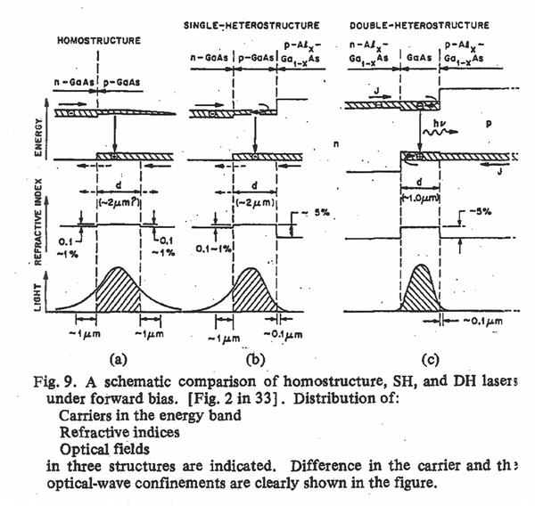
Izuo Hayashi of BTL and others devised a gallium-arsenide/aluminum-gallium-arsenide double-heterostructure laser and succeeded in CW laser operation at room temperature.
Corning started selling the low-loss quartz optical fiber invented by Charles K. Kao. The emergence at about the same time of both a light source and light conducting medium launched the evolution of optical communications.
1974: Release of a commercial low-noise gallium-arsenide MESFET (NEC)
The gallium-arsenide metal?semiconductor field effect transistor (MESFET) was proposed by C. A. Mead in 1966. As electrons are several times more mobile in gallium arsenide than in silicon and also as semi-insulating substrates can be made of gallium arsenide, the gallium-arsenide MESFET held promise as a high-frequency transistor. More than 30 companies worldwide developed MESFETs. Of these, NEC developed superior technologies for growing crystals and forming electrodes, and released the world’s first commercial low-noise gallium-arsenide MESFET for microwave-band wireless communication.
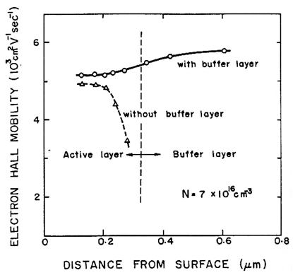
Electron Mobility Profile of Vapor-Phase Epitaxial Growth Layer
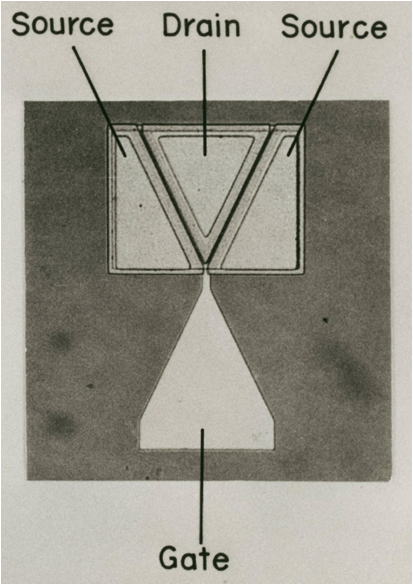
Die of Noise-Reduction GaAs MESFET with 1-mm Gate
1974: Development of an aluminum-gate power MOSFET for the UHF band (Fujitsu)
Up to this stage, silicon bipolar transistors were used for large-output amplification in the UHF band. Y. Morita of Fujitsu developed an aluminum-gate nMOSFET with a gate length of 5 μm (and a gate width of 20 mm) and succeeded in obtaining 16 W of output power and a gain of 6 dB at a frequency of 700 MHz. This was the world’s first demonstration of the advantages of using MOSFETs in the UHF and microwave bands.
1974: Release of a commercial audio amplifier employing a static induction transistor (SIT) (Yamaha Corporation)
In 1950, Jun-ichi Nishizawa of Tohoku University developed the static induction transistor (SIT). Its triodic characteristics enabled the development of an SIT for audio amplifiers. Yamaha used the SIT in the commercial B-1 audio amplifier (150 W of output power) released in 1974.
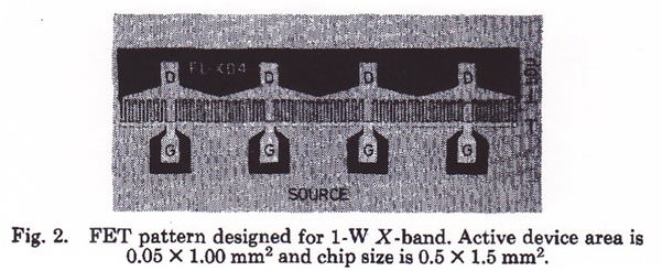
1975: Release of a commercial large-output GaAs MESFET (Fujitsu)
Focusing on the high-frequency large-output capability of the gallium-arsenide MESFET, Fujitsu released the world’s first commercial microwave-band large-output gallium-arsenide MESFETs. Special processes were used to ground the source and form the electrodes. They replaced the traveling-wave tube (TWT), which until then had been used for C- and X- band microwave link equipment, and thus enabled the world’s first all-solid-state microwave link equipment. Adopted in amplifiers for satellite communications in 1989, the MESFET is still widely used in microwave-band applications.
1975-85: Improvement of photodiode for image sensor (Sony, Hitachi, NEC, Toshiba)
Photodiodes for image sensors were significantly improved and developed around 1980. This is termed “Pinned Photodiode” and has been used in most CCD and CMOS image sensors since the 1990s.
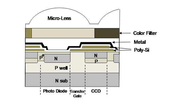
Fig-1 Recent Image Sensor with Pinned Photodiode
1978: Release of a commercial gallium-arsenide/aluminum-gallium-arsenide semiconductor laser (Hitachi and Mitsubishi Electric)
The semiconductor laser, for which CW oscillation at room temperature was achieved in 1970, had the disadvantages of a very short lifetime and unstable oscillation modes. Hitachi and Mitsubishi investigated the reasons for the rapid deterioration, developed technologies to alleviate this problem, and invented structures that enabled stable oscillation modes: the channeled substrate planar (CSP) and buried heterostructure (BH) types from Hitachi and the transverse junction stripe (TJS) type from Mitsubishi. Through these advances, the two became the first companies in the world to sell semiconductor laser diodes.
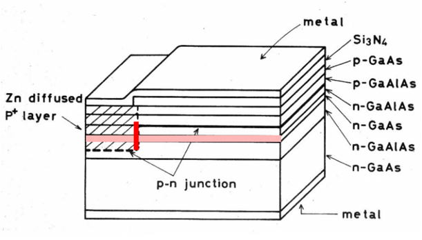
Cross-Sectional Structure of TJS Laser
1978: Development of a commercial 110,000-pixel CCD image sensor (Sony)
Activity towards developing CCD image sensors with the aim of replacing image pickup tubes accelerated from about 1975. Sony led the world in 1978 by releasing a commercial 2/3” 110,000-pixel (242H × 490V) CCD image sensor, the ICX008. In 1980, Sony started selling the XC-1 color camera, in which two of these CCD image sensor chips were used.
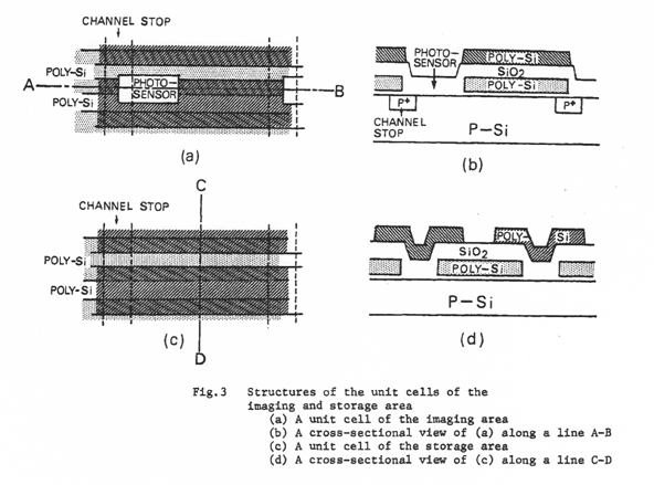
Structure of 110,000-pixel CCD Image Sensor
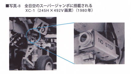
XC-1 (pixels: 245H ´ 492V) in All Nippon Airways Co., Ltd.’s Superjumbo Jet (1980)
November 1979 to August 1980: Development of a 1.3-μm-band semiconductor laser (NEC, Hitachi, and Fujitsu)
The first commercial quartz fibers showed the least loss at a wavelength of about 850 nm. As fiber fabrication technology advanced and the purity of the quartz increased, the wavelength showing the least loss shifted up, first to 1310 nm and then to 1550 nm. This led many manufacturers to start developing indium-gallium-arsenide-phosphide/indium-phosphide-based lasers.
The Tokyo Institute of Technology and the Nippon Telegraph and Telephone Corporation achieved continuous operation of an indium-gallium-arsenide-phosphide/indium-phosphide-based laser in 1976. After that, many manufacturers successfully developed 1.3-μm-band indium-gallium-arsenide-phosphide/ indium- phosphide-based semiconductor lasers featuring low oscillation thresholds, and this led to the start of F-400M operations by NTT in December 1983.
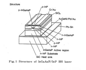
Structure of InGaAsP/InP BH laser
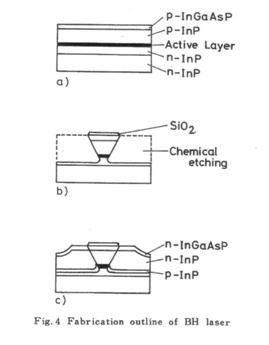
Fabrication outline of BH Laser
1979: Invention of the HEMT (Fujitsu)
The high electron-mobility transistor (HEMT), a kind of field-effect transistor in which a two-dimensional electron gas on the semiconductor heterojunction interface serves as the channel, was invented by Takashi Mimura of Fujitsu Laboratories in December 1979. Due to their fast operation at high frequencies, HEMTs were used in the low-noise receiver of the radio telescope of the National Astronomical Observatory in 1985 as a first step towards commercial use. The device is now regarded as important for applications such as satellite broadcasting and mobile radio communications within the microwave and millimeter-wave communications fields. This invention was also important in focusing attention on the significance of various semiconductor heterojunctions.
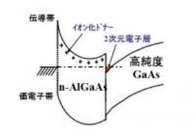
Band structure of HEMT
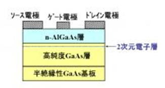
Outlined structure of HEMT