
Process Technology
1970s
The 1970s was an age in which innovation in process technology changed from the question of whether a device could be made to the question of how to make a more advanced device.
Though variety of manufacturing equipment still had to be imported, the transition to domestically produced equipment was just getting under way based on advice from the VLSI Technology Research Association and the individual companies.
Early 1970s: Using low-pressure CVD to form films of polycrystalline silicon, oxide, and silicon nitride
Instead of normal-pressure CVD equipment in which the wafers were placed horizontally, horizontal diffusion furnaces were introduced to achieve a technique for creating silicon gates. Within the furnace, polycrystalline silicon was applied within a process tube under reduced pressure. Low-pressure CVD equipment which was also capable of applying silicon nitride was used to implement a local oxidation of silicon (LOCOS) technique.
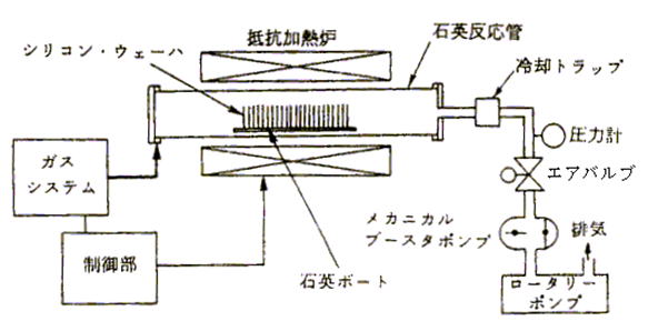
Structure of Low-Pressure CVD Equipment
Early 1970s: Control of threshold levels by ion implantation
Medium-current ion implanters began to be used to control the threshold levels of MOS transistors and to prevent inversion in isolation areas. The mainstream of manufacturers of the required equipment was overseas manufacturers such as Lintott Control Systems Limited.
1970s: Usage of reflow in a flattening technique
Heating a highly-concentrated phosphosilicate glass (PSG) to melting point was used to flatten rippled surfaces. This prevented the disconnection of aluminum wiring due to surface unevenness. At the end of the 1970s, BPSG, made by adding boron (B) to PSG, was also being used.
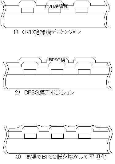
Flattering Technique by BPSG Reflow Process
Mid-1970s: Lithography technique moves from contact exposure to proximity exposure
Lithography techniques had made progress by the middle of the 1970s, with the form of exposure changing from contact to proximity, masks changing from emulsion masks to hard masks, and photoresist changing from photographically negative to positive. Japanese manufacturers such as Canon Inc., Tokyo Ohka Kogyo Co., Ltd., and the JSR Corporation began to emerge as leading companies in terms of equipment and materials.
Proximity Exposure Equipment: PLA-300
Auto Alignment Proximity Exposure Equipment: PLA-501FA
Around 1975: Introduction of aluminum–silicon sputtered wiring
Equipment that applied sputtering instead of evaporation in the deposition of thin metal films was produced around 1975. This led to the use of aluminum–silicon, for its stronger robustness against connections breaking, instead of aluminum as the wiring metal.
Late 1970s: Usage of isotropic plasma etching
Although chemicals were initially used to pattern silicon gates, isotropic plasma etching equipment eventually came to be used instead. Manufacturers of such equipment were Tokuda Seisakusho Co., Ltd. (chemical dry etching equipment), the Tegal Corporation, and Tokyo Ohka.
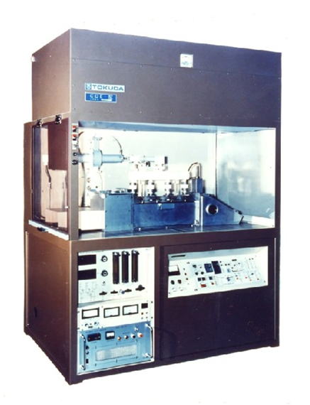
Chemical Dry Etching Equipment: CDE-4
Late 1970s: Appearance of projection aligners for lithography
As a further advance in miniaturization, new projection exposure equipment replaced contact and proximity exposure equipment. In one trend, exposure equipment of x1 magnification from PerkinElmer Co., Ltd. and Canon was entering service. In another trend, GCA Corporation started to sell steppers. Nikon Corporation delivered a prototype stepper to the VLSI Technology Research Association.
First Domestic Projection Aligner