
Integrated Circuits
2000s
Decade of LSI as infrastructureDuring this decade, LSI circuits were embedded in almost all electronic devices and the most device functions came to be realized by LSIs. Semiconductors provided an indispensable infrastructure for electronic devices, and the platform development approaches (software and hardware as a unit) spread. As a wider variety of functions were implemented in each electronic device, product planning and marketing skills to determine what types of LSI circuits should be developed became increasingly important, as well as the ability to develop the technology itself.
2000s: Flash memory business in full fledge.
Progress in microfabrication and multi-level technology enabled rapid increases in NAND flash memory capacity, and when this reached 1 Gbit, it overtook the capacity of DRAM at the time. By 2010, 64-Gbit flash memory was being mass-produced. As capacities increased, the fields of application for flash memory expanded to encompass digital cameras, portable audio/video players, mobile phones, and USB memory, and flash memory business reached its height of prosperity.
2000s: Larger-scale systems on SoCs
Since 2000, the increased scale of systems needed for mobile phones, digital TV sets, and car navigation systems caused a huge increase in the size of integrated SoC systems, which went from 10 million gates to several tens of millions of gates. Not only did the SoC hardware grow, the related software also grew in a similar way. The efficient development of such huge systems became a major issue. To deal with this, the platform development approach was refined.
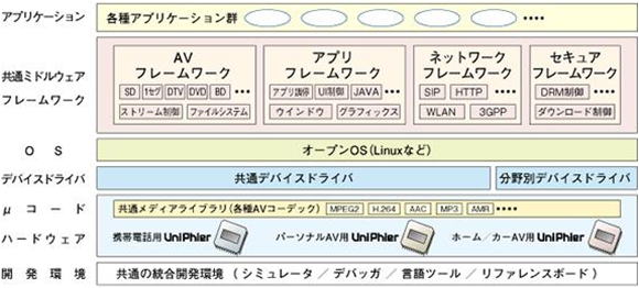
Commonalization of Software Architecture in UniPhier 1)

Commonalization of Hardware Architecture in UniPhier 1)
2000s: Development of new types of memory
New types of nonvolatile memory – such as magnetoresistive memory (MRAM: magnetoresistive RAM), phase change memory using chalcogenide (PCRAM: phase change RAM), and resistance-change memory (ReRAM: resistance RAM) – were proposed and developed.
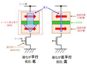
Operating Principle of MRAM
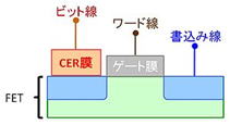
FeRAM Structure
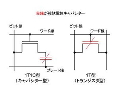
FeRAM Structure
2000s: Enhanced interlinkage between design and production
To cope with the increased difficulty of fabrication due to enhanced miniaturization, technologies for interlinkage between design and production were developed. One such was the design-for- manufacturability (DFM) technology, which fed acquired know-how concerning ways to improve yield, with the know-how defined as rules, back to the chip design process. Others included design-for-testability (DFT) technologies, such as boundary scan or BIST technology, which facilitate testing.
2000s: Exploring New Structure Devices
In 2000, researches on various new device structures have been actively carried out with the perspective that conventional planar type MOS transistor structures will face the miniaturization limit soon. These structures include UTB (Ultra-thin body) SOI structure, FINFET, Multi-gate transistor, etc. Studies of pursuing the possibilities of device operations using entirely new materials such as carbon nanotube, graphene, etc. have also been carried out.
2001: Release of LSI with embedded FeRAM for IC cards (Fujitsu and Matsushita)
The release of ferroelectric RAM (FeRAM) – a new memory different from DRAM, SRAM, or flash memory – was preceded by a long period of basic study and development aimed at ferroelectric materials. After Rohm, Matsushita, and Fujitsu each released an FeRAM memory (FRAM), Fujitsu released an LSI circuit with embedded FeRAM for IC cards in 2001. This was followed by Matsushita (now Panasonic) releasing its own LSI circuit with embedded FeRAM for IC cards in 2003.
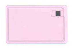
IC Card with Embedded FeRAM by Fujitsu Limited
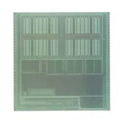
LSI for IC Cards with Embedded FeRAM by Fujitsu Limited
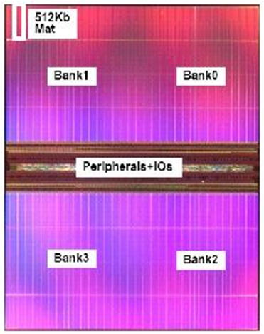
128-Mbit FeRAM by Toshiba Corporation
2003 : Development of First-generation Visconti™ T5BG3XBG Image Recognition Processor (Toshiba)
Toshiba developed Visconti™ first generation T5BG3XBG image recognition processor. This product is a multicore processor equipped with 3 MPE (Media Processing Engine) cores composed of RISC (Reduced Instruction Set Computer) and VLIW (Very Long Instruction Word) core and image processing accelerator, and it was developed for the application to advanced driver assistance system (ADAS)
2005: Cell Broadband Engine™ (group consisting of Toshiba, IBM, and Sony Corporation)
Toshiba, IBM, and Sony jointly developed the Cell Broadband Engine (Cell B.E.). The Cell B.E. is a multi-core processor providing high-level functionality for parallel operations through a 64-bit general core based on the PowerPC architecture and eight 128-bit multimedia processing cores. The Cell B.E. is incorporated in the PlayStation3 video game console from Sony and then in digital TV sets from Toshiba (Cell REGZA). It is also incorporated in IBM’s Roadrunner supercomputer.
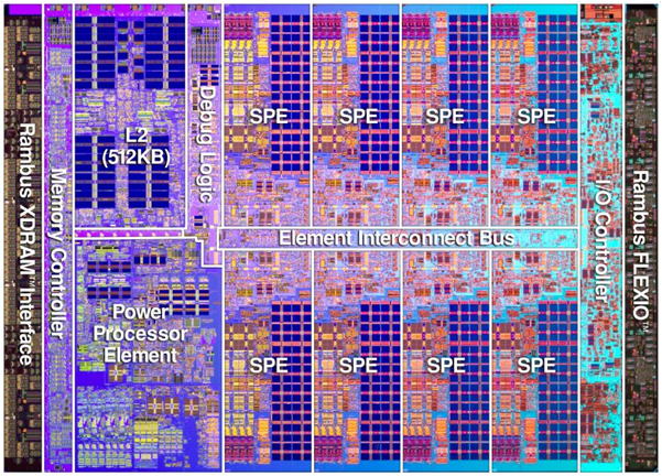
Die Photo of the Cell/B.E.
Late 2000s: Shift to multi-core processors
Improvements in processor performance had generally been achieved by raising operating frequencies. However, this technique came up against limits due to the increased power consumption by chips. Multi-core configurations were devised as a new kind of solution where multiple processor cores are integrated on a single chip.
This enables both high performance and low power consumption through operation of the multiple cores in parallel. Following on from IBM’s release of the POWER4 microprocessor, Intel developed the Pentium Extreme Edition 840 processor and Core Duo processor for personal computers. In Japan, Renesas Technology developed the dual-core SH2A and SH4A, and NEC Electronics developed the V850E2M.