
Equipment & Material
1990’s
Entering the deep submicron era, the wafer size was enlarged to 8 inches (200 mm). Standardization of manufacturing equipment as the platform for entire semiconductor industry became international consensus, and its standardization progressed. Meanwhile, SiP (System in Package) became important, and the requirement for new packaging materials increased.
Early 1990s: i-line reduction-projection exposure system
The g-line reduction- projection exposure system, which became the main equipment in the 1.3 to 0.8 μm process generation, shifted to the i-line reduction- projection exposure system in the 0.5 to 0.35 μm generation in the 1990s.
1990s: Low-k dielectric materials
SiO2, which was used as an insulating film between interconnections in LSIs, began to be replaced by low-k materials with low dielectric constants in order to reduce the capacitance between wirings as miniaturization progressed in the 1990s.
1994: One-bath wafer cleaning system
One-bath batch cleaning system appeared in which a series of wafer cleaning process was treated in single bath by changing chemicals and deionized water for rinse in 1994. The system replaced the conventional multi-bath system that had been used until then. This led to an ultra-clean, space-saving, and energy-efficient cleaning process.
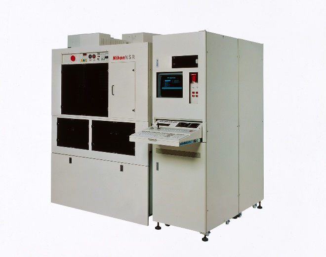
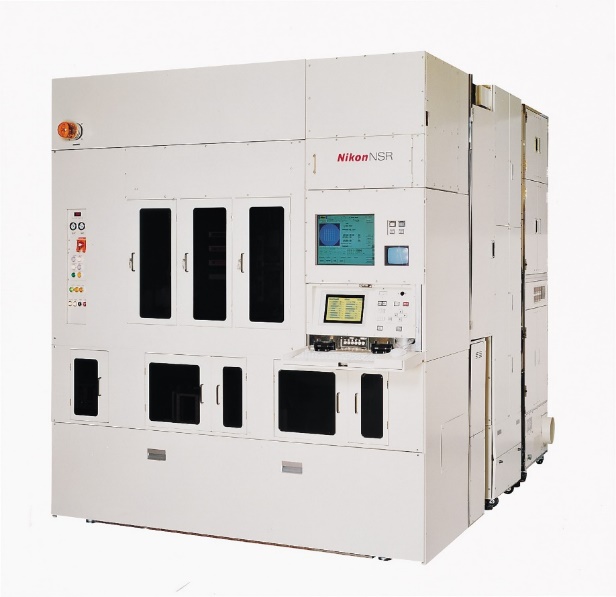
Late 1990s: KrF excimer laser step-and-scan exposure system
The KrF excimer laser scanner system was established as an exposure system for the deep-submicron region, replacing the conventional stepper in the latter half of the 1990s.
1990s: Chemical amplification photoresist
Chemical amplification photoresist was realized, so that lithography technology using the KrF excimer laser was launched in the latter half of the 1990s. Chemical amplification photoresists became indispensable for later ArF and EUV lithography.
1990s: Establishment on supply chain for CMP system and materials
The supply chain of CMP system and related materials was established, and STI (Shallow Trench Isolation) and Cu damascene interconnections became widespread as standard technologies in the 1990s,.
1990s: SMIF for wafer transfer
The SMIF system, in which wafers were enclosed in sealed storage pods, conveyed between process steps, and transferred to and from the manufacturing equipment through load ports, began to be adopted in the 1990s. This system became the standard for 300 mm wafer processes since the 2000s.
Late 1990s: 300mm Standardization Activities
International standardization activities for manufacturing equipment and materials proceeded as process evolved toward the 300 mm wafers in the latter half of the 1990s. This had a significant effect in increasing flexibility in equipment and materials procurement for device manufacturers and reducing development and manufacturing costs for equipment and material suppliers.
1998: Issue of ITRS
International Technology Roadmap for Semiconductors (ITRS) was published in 1998. It became a valuable guideline for the semiconductor manufacturing equipment and materials industry.
1990s: Build-up material
Ajinomoto Fine-Techno's ABF became the global standard for build-up materials used as the insulating layer for wirings in SiP modules.