
Equipment & Material
1970’s
Technological innovation of advanced processes that follows the scaling rule was advanced by collaboration between device manufacturers and manufacturing equipment/material suppliers. Especially in Japan in 1976, the VLSI Technology Research Association was established and cooperative development of manufacturing equipment and materials was promoted as a common basis of the semiconductor industry.
1970: The Launch of SEMI
SEMI was established in 1970 and since that time, the industry group activities towards the establishment and development of an international supply chain between semiconductor device manufacturers and equipment and material manufacturers were advanced.
1970's: RCA Cleaning
RCA cleaning was announced in 1970. RCA cleaning has become a standard cleaning method in semiconductor processes and has been widely used in the world for over 40 years.
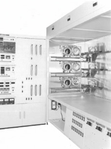
1970's: Low Pressure CVD (LPCVD) Equipment
Low pressure CVD (LPCVD) method was announced from Fujitsu in 1971, and low-pressure CVD equipment began to be produced and sold in the mid 1970’ s. Film uniformity and step coverage of Poly-Si, Si3N4, SiO2 and the like are greatly improved, making it essential for miniaturization and high integration of semiconductors.
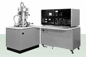
1970's: Field Emission Scanning Electron Microscope (FE-SEM)
Hitachi (currently Hitachi High-Tech Corporation) developed FE-SEM in 1972. SEM is an indispensable tool for LSI device and process development, since reduction of micro defects limits the yield and reliability of LSI.
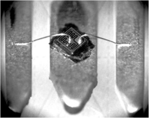
1973: Automatic Wire Bonding Equipment (AWE)
In 1973, fully automatic transistor assembly robot was developed. This device is called AWE (Automatic Wire-bonder with Eye), which automated the manual work that required 1000 operators per factory, who were also called transistor girls.
1970's: Proximity Aligner and Projection Aligner
In the 1970's, the lithography technology of LSI that had begun with the contact exposure method was replaced by proximity exposure method and projection exposure method in order to improve resolution of fine patterns and to reduce defect density. In addition, an automatic positioning mechanism was provided to drastically improve productivity.
Late 1970's:Positive Photoresist
In the latter half of the 1970's, the proximity exposure method and the projection exposure method became the mainstream of photolithography instead of the contact exposure method. At the same time, positive photoresists came to be widely used instead of negative photoresists used in the contact exposure method.
1970's: Polyimide Resin
In the late 1970s, polyimide resin, which is an organic material, was introduced into the interconnect interlayer insulating film and the protective film of the chip. After that, the polyimide resin became one of the structural material which is indispensable for LSI manufacturing
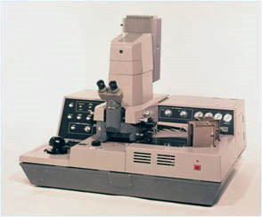
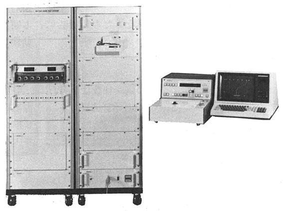
1970's: Linear IC Tester
In 1974, Shibasoku launched the first domestic linear IC tester. It was the beginning of the domestic linear IC tester.
1978: Reactive Ion Etching (RIE) Equipment
In 1978 Nichiden Anelva (now Canon ANELVA) developed a reactive ion etching (RIE) equipment. This method enabled the anisotropic etching which realized the precise etched dimensions to the resist mask and became the mainstream of the current etching method.
1978: Reduction Projection Exposure System (Stepper)
In 1978, a reduction projection exposure apparatus (stepper) appeared. In this year, GCA started selling 10:1 stepper. In the same year Nikon also delivered a 10:1 stepper to Ultra LSI Research Association. This is the beginning of the reduction projection wafer exposure.
1970's: Electron Beam Lithography System
As a candidate for fine pattern formation method to replace light exposure, development of electron beam lithography had been advanced in the world from the 1970 's. Although this system was used for production of LSIs of many kinds and small quantities, the productivity was low and it was not suitable for general purpose LSI production. On the other hand, in the production of photomasks and reticles, pattern generators based on optical method had limitations in productivity due to the exponential increase in the number of patterns due to miniaturization, and electron beam lithography capable of high-speed pattern generation became indispensable.