
Packaging Technology
Changes in Package Shapes of ICs and LSI devices
2000s
2000s: Era of the three-dimensional stacked mounting SiP (system in package)The strength of the U.S. was in high density monolithic SoCs. In contrast, Japan focused also on the importance of three-dimensional stacked mounting techniques to enable system-LSI devices development in short periods and with low cost. SiP technology and module mounting technology evolved through the cooperation with the material and equipment manufacturers, and these technologies contributed to realize multiplication of the functions of information terminals (e.g. cellular phones) and the system-mounting of motor-driving units.
2000: Development of the LFPAK(R) low-inductance transistor package
Hitachi developed the LFPAK(R) as a structure that lowered the inductance of wire bonding. Gold-wire stud bumps are formed on the device and the lead frame is placed on them. This package is used for power MOS devices to drive Li-ion battery systems as a measure to extend battery life.
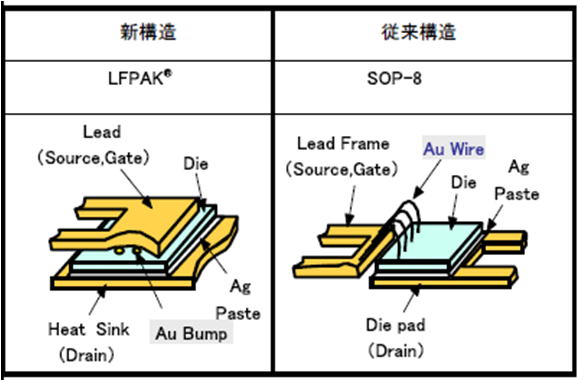
LFPAK Compared with Conventional SOP
2000: Development of a PAM for multi-channel radio communication
Murata Manufacturing Co., Ltd. actively developed power-amplifier modules (PAMs) in which all system circuits of a baseband unit (the bandpass filter, bypass capacitor, and impedance matching unit) are integrated. This was done by using the LTCC (low-temperature co-fired ceramic) technique. PAMs can be used for communications over many channels, allowing the connection of cellular phones to the Internet, and usable in global communication environment, and so on.
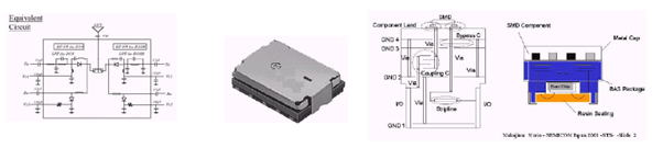
PAM (Power Amplifier Module) by Low Temperature Co-fired Ceramic Technique
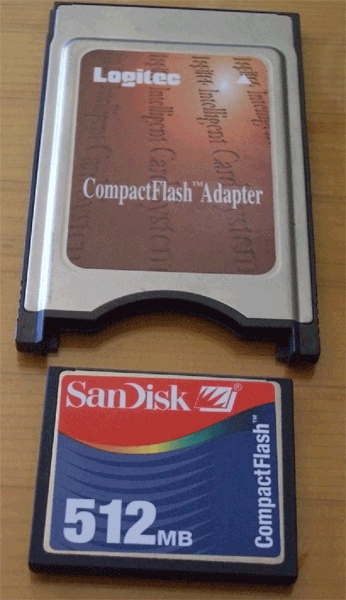
Around 2000: Birth of various flash cards
With the appearance of large-capacity NAND flash-memory devices for the storage of digital data, many models of flash cards were developed as external semiconductor memory cards for such electronic information appliances as personal computers. Flash cards for use by consumers take many forms, including compact flash memory, multimedia cards, memory sticks, SD cards, micro-SD cards, and USB memory sticks.
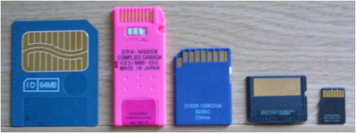
Various Types of Flash Memory Cards
2002: Usage of first SiP product in a digital camera
Renesas Technology Corp. established the SiP (system in package) design technique in which a system LSI is implemented by mounting different types of device (for example, memory devices) on top of an MPU device. This technique was first adopted in digital still cameras. In comparison with an SoC (system on chip) design, in which all of the circuits are formed on the same piece of silicon, an SiP design has such advantages as shorter development periods, lower development costs, and ease of incorporating high density memory. The SiP technique has been adopted for digital cameras and cellular phones, and its high noise tolerance has enabled its further applications in automobiles, medical devices, and image transfer.
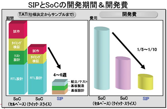
Development Periods and Cost Comparison of SoC and SIP
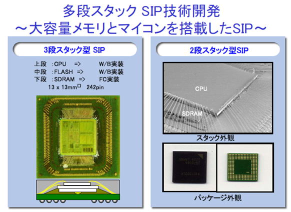
Chip-Stack SIP with Large Density Memory and MCU
2002: Expanded mass production of power semiconductor modules for inverters
Mitsubishi Electric Corporation expanded its mass production of power modules containing integrated motor-driving systems. Several semiconductor devices, including IGBTs, backflow prevention diodes, and a microcontroller, are mounted on a single lead frame in each such module, The device is completed as a pin-insertion type package, after aluminum wire interconnect and transfer molding. Mitsubishi calls the modules of this type DIPIPMsTM (dual in-line package intelligent power modules).
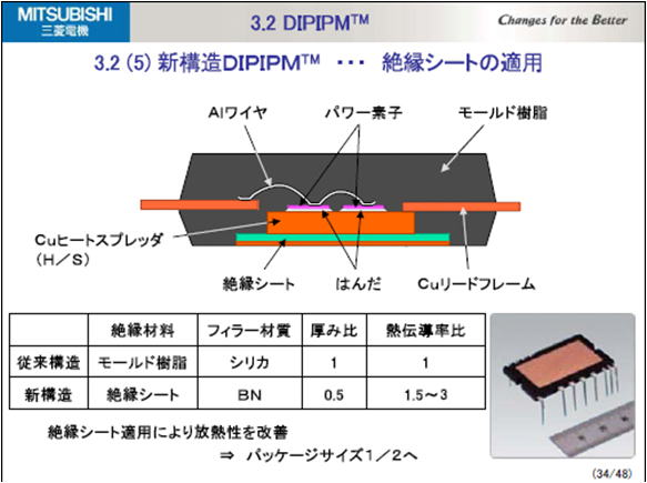
Improved Structure of DIPIPM
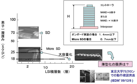
2005: Enhancement of multi-layer stacking in micro-SD cards
Further size reduction and capacity increase of NAND Flash memory systems were pursued, in order to store full-color photographic image data in handheld electronic equipment like digital cameras and cellular phones. Multi-layer stacking of thin wafers/dies to be applied to high-density SSD (Solid-state Drive) for note-PC applications and micro-SD for mobile phones was further enhanced, with the advanced back-grinding technique to realize ultra-thinning of wafers. 8, 16, and then 32 layer stacking were successively realized.
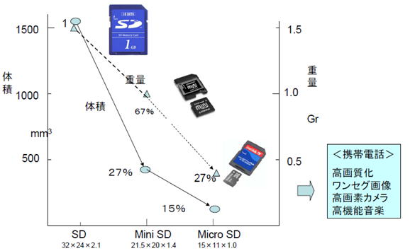
Volume of Various Types of SD Cards
Die Thickness and Number of Die Layers of Stacked LSI Module
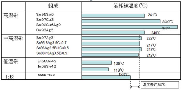
2005: Accelerated switchover to lead-free solder in response to Europe’s RoHS directive
As one of the measures to global environmental issues, the use of lead-free solder materials was promoted in the European market as a solution under the RoHS (Restriction of Hazardous Substances) directive. Japan recommended tin-silver-copper materials and applied them in mass production.
Various Lead-free Solder Materials
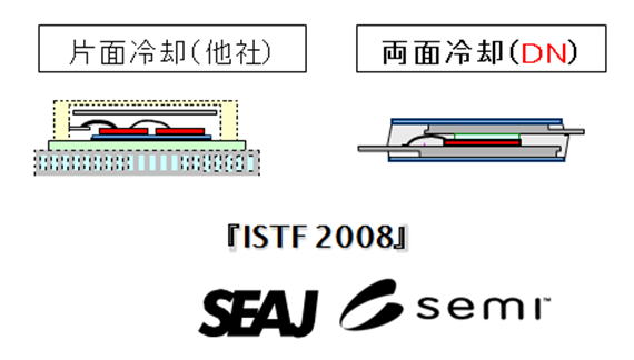
2007: Development of power-card techniques for driving the motors of HEVs
The Toyota Motor Corporation and Denso Corporation actively developed new packages to reduce the power consumption of motor driving units and power supply units in hybrid electric vehicles (HEVs) and electric vehicles (EVs). Instead of aluminum-wire bonding, the semiconductor device is sandwiched within a copper lead frame that is highly conductive for both heat and electricity in the so-called clip-lead structure. This realizes a combination of low inductance, low resistance, and good heat dissipation. Application of this structure in products is expanding.
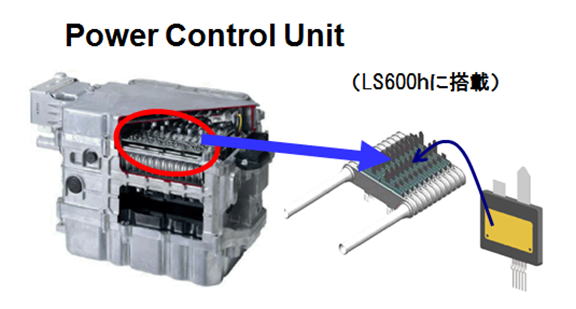
Power-cards and its Mounting to Power Control Unit
2009: Release of DRAM memory modules using TSV
Elpida Memory, Inc. announced its application of TSV (through-silicon via) technology in DRAM memory modules. DIMM (dual inline memory module), SO DIMM (small-outline DIMM), and micro-DIMM were developed in turn in 8-chip stacking by TSV technology of hole filling by poly-silicon and then solder joining.
i-308,309
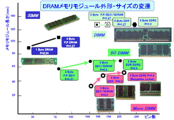
Changes of Shape and Size of DRAM Modules
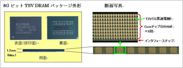
8Gb Stacked DRAM by TSV Technology
2010s
2010s: Era of MiP (multiple functions in a package)The evolution of semiconductor packaging technology towards incorporation of multi-faceted functionality is predicted, enabling the control of not just electrons but also electromagnetic waves in the radio frequency (RF) and visual light (photons) bands.