
Process Technology
2000s
The 2000s was an era in which the limits of miniaturization presented challenges. At the same time, semiconductor devices were applied in a large variety of products constituting the core products of Japanese industry.
The diameter of wafers was enlarged to 300 mm and investments greater than a thousand million dollars per factory came to be required. Such enormous investments intensified the trend towards oligopoly and contributed to the conflict between overcoming the challenges of miniaturization and increasing costs.
Early 2000s: Transition to 300-mm wafers
The change in wafer diameter from 200 mm to 300 mm did not lead to as much trouble in the industry as the change to 200-mm wafers, but imposed a larger share of development costs on the equipment industry.
2000s: Change of the light source for exposing equipment to argon-fluoride excimer lasers and expanded application of liquid immersion of lenses
To cope with miniaturization to feature sizes below 250 nm, the argon-fluoride excimer laser, producing a wavelength of 193 nm, was adopted as the light source for exposing equipment. However, there was no practicable way of further shortening the wavelength of the light source. Instead, the substitute for exposing equipment was a technique where the lens was immersed in water to obtain an NA above one.
ASML in the Netherlands had emerged as an equipment manufacturer, joining Japan’s Nikon and Canon.
2000s: Sophisticated resolution techniques
The wavelength of the light source for the exposing equipment was not shortened beyond 193 nm. To further compensate for this, complex optical proximity correction (OPC) processing was applied to the mask or a double-patterning technique was about to be used. This significantly raised the costs of masks.
2000s: Adoption of low-permittivity (k) materials for the films between interconnect layers
Miniaturization increased the signal delay caused by interconnect. A solution was to change the insulation film between interconnect layers to a low-permittivity material. However, when a low-k material with a relative permittivity of 3 or less was used, the formation of copper interconnect by the damascene method now required a metal to serve as a barrier or seed layer. Thus, both low-pressure CVD equipment for flattening the low-k film and sputtering equipment or ALD equipment for depositing the barrier or seed layer were also necessary.
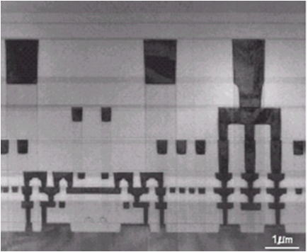
Example of Cross-Sectional Views of Cu Multilayer Interconnection Using Low-k Materials
2000s:ALD (Atomic Layer Deposition)
ALD was invented by Tuomo Suntola in Finland in 1974. It was applied to the film formation method of ZnS for EL (Electro Luminescence), and was then developed in various fields. In the semiconductor field, it was applied to GaAs growth method called MBE (molecular layer epitaxy) by Tohoku University. In the field of silicon semiconductors, it became a deposition method indispensable for miniaturization after the 90 nm node.
Late 2000s: Usage of strained silicon for high-speed transistors
Independently of miniaturization, the use of strained silicon techniques to increase the speed of transistors commenced. The techniques involved applying a liner film to impose internal strain or locally implanting germanium in the silicon.
Late 2000s: Adoption of high-k materials and metal gates for high-speed transistors
For effective reductions in the thickness of gate insulation films and increased speed for the transistors of the most advanced logic LSIs, insulation films are formed of a high-k substance (e.g. hafnia) and the gate electrode substance is changed from silicon to metal (made from different raw materials from the old aluminum gates).