
Process Technology
1960s
This decade was an age of imitation of U.S. technologies. At first, equipment produced in-house was the mainstream in semiconductor manufacturing. In this situation, some equipment manufacturers then started to provide manufacturing equipment in response to requests from other companies.
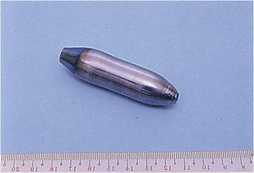
Single Crystal Ingot of Silicon Created by Toshiba Corporation’s Czochralski Pulling Equipment in 1956
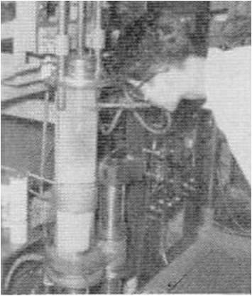
Example of Czochralski Pulling Equipment Made In-House(Toshiba Corporation)
Early 1960s: Start of using the CZ method to manufacture crystal silicon for silicon transistors
The manufacture of silicon transistors started in the 1960s, and each of the companies involved made its own Czochralski pulling equipment to create single crystals of silicon through the CZ method. Japanese metal material suppliers also started manufacturing and selling polycrystalline silicon, the raw material for single-crystal silicon.
Early 1960s: Using an epitaxial technique to manufacture silicon transistors
Silicon transistors were made by forming a lightly-doped epitaxial layer on top of a heavily-doped substrate (n+ or p+). To manufacture silicon transistors, companies made their own epitaxial equipment, optimized the process conditions, and handled epitaxial growth in-house.
Early 1960s: Transition to thermal oxidation and vapor-phase diffusion by horizontal diffusion furnaces
Fabricating silicon transistors using a planar technique required oxidation of the silicon surface, opening apertures in the oxide film thus formed, and the formation of p-n junctions by vapor-phase diffusion through the apertures.
A horizontal-type furnace was used for oxidation and diffusion.
Although the diffusion furnaces were initially made in-house, commercialized products from Hitachi Kokusai Electric Inc. were made available from the middle of the 1960s.
1960s: Using thin films of evaporated aluminum to form electrodes and wiring
Thin films of aluminum were used to bring semiconductor terminals into contact with electrodes in silicon transistors. ICs entered mass production in the late 1960s, and the films were also used here to form wiring between the transistors.
Resistive heating was initially used to evaporate the aluminum for forming thin films, but electron beams came to be used for this purpose in the 1970s.
1960s: Manufacture of silicon devices by using contact lithography
A lithographic (photolithographic) technique was used to make patterns and to open the apertures in oxide film and then make patterns of thin aluminum films in the manufacture of silicon transistors and ICs. The method used in the 1960s was contact lithography where an emulsion mask was pressed to the wafer, which was then exposed.
Late 1960s: Formation of oxide films by normal-pressure CVD
In the late 1960s, the creation of oxide films through chemical synthesis by using normal-pressure chemical vapor deposition (CVD) equipment became possible alongside the creation of films by thermal oxidization. Such oxide films came to be used as protective films over the electrodes and wiring. Both commercially available equipment and equipment made in-house were used in this process.
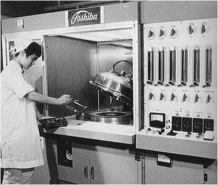
Normal-Pressure CVD Equipment Manufactured In-House
Late 1960s: Application of CVD oxide films for low noise device process
Both using CVD oxide films, Hitachi, Ltd. developed the low-temperature passivation (LTP) technology and the Toshiba Corporation developed the perfect crystal technology (PCT) for low-noise transistors and ICs for audio applications.
This expedited progress in converting the circuits of Japanese consumer equipment to the solid state (semiconductors)
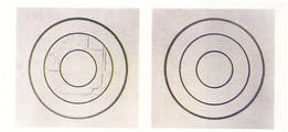
Reduction of Crystalline Defects by PCT