
Process Technology
1980s
The 1980s was an age in which Japanese companies and equipment manufacturers began to win quality and manufacturing yield competitions. Variety of manufacturing equipment was produced domestically, and both the device and equipment businesses grew larger due to completely automated processes, a speciality of Japan. Meanwhile, the large growth became an target of attack in trade friction between Japan and the U.S. This age was also the beginning of the road to difficulties in later times.
Early 1980s: Advancing miniaturization requires the use of steppers in lithography
Projection aligners of x1 magnification were used until the beginning of the 1980s. However, after commercial steppers by Nikon and Canon became available in 1980 and 1984, respectively, steppers became the mainstream.
Furthermore, the subsequent evolution of steppers allowed miniaturization to proceed in accord with industry road maps.
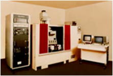
Vertical diffusion furnace
Early 1980s: Introduction of anisotropic plasma etching equipment (RIE)
As a further advance in miniaturization, anisotropic plasma etching equipment (RIE) began to replace isotropic plasma etching equipment.
Early 1980s: Transition to formation of diffusion layers by ion implantation
Depths of diffusion had to be made shallower for yet further miniaturization. Instead of using the conventional thermal diffusion method to form junctions, a new method of implanting impurities by ion implantation with subsequent heat treatment was used.
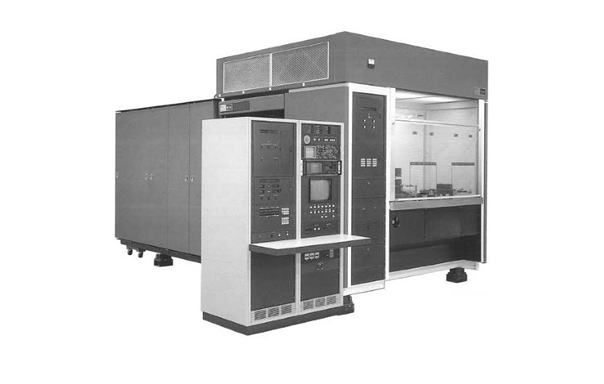
Schematic of ECR (Electron-Cyclotron Resonance)-CVD
Middle of 1980s: Transition of flattening technique from reflow to etching back
An etchback method, in which global etching of a wafer is applied by plasma etching equipment after application of photoresist, replaced the reflow method. This not only improved the flatness but at the same time lowered the temperature of the process, thus enabling an increase in the number of interconnect layers.
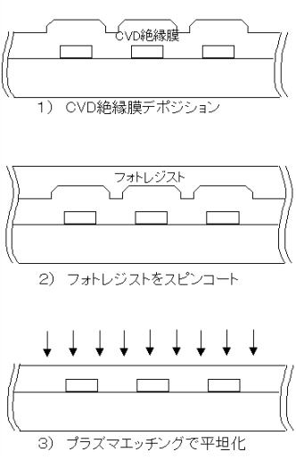
Flattering Process by Etchback
1980s: Plasma CVD (of low-temperature SiO2/SiN) becomes the mainstream
In the 1980s, as the temperatures of processes had to be lowered along with advances in miniaturization, plasma was used in the CVD to deposit films of silicon dioxide and silicon nitride at lower temperatures.
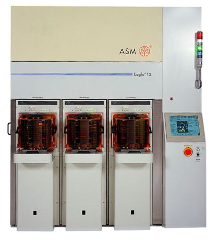
12" Single Wafer Plasma CVD Equipment by ASM Japan
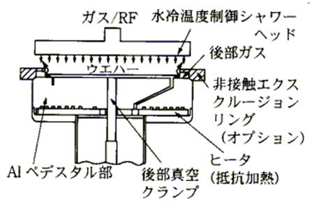
Example of Chamber Structure of Plasma CVD Equipment
Late 1980s: Applying three-dimensional cell structures to DRAM
As the integration of DRAM increased, three-dimensional memory cell structures were adopted for reduced cell size. Specifically, the three-dimensional cell structures were a trench cell and a stacked cell, and both were invented in Japan in the 1970s. The hemispherical-grained polysilicon technique which was used to further miniaturize the stacked cell was also originated in Japan.
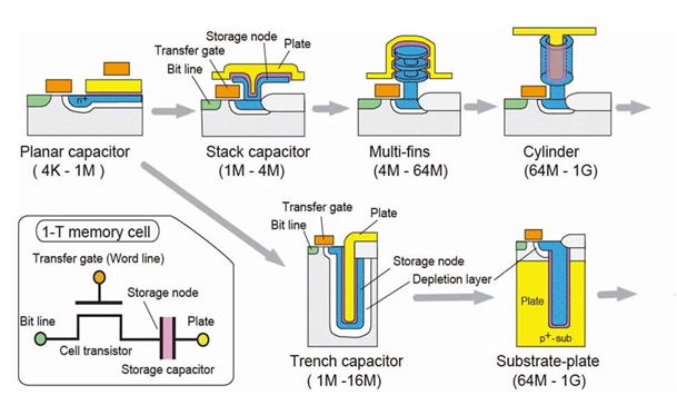
Three-Dimensional Cell Structuring in DRAM
Late 1980s: Using a sputtering technique for silicide gates
Silicide gates came into use for reducing resistances at silicon gate electrode. Since the CVD of silicide films was not possible, silicide films were formed by sputtering.
1980s:Formation of Deep Well by High Energy Ion Implantation
With the development of ion implantation technology, high energy ion implantation became possible. As a result, it became possible to form various kinds of wells in LSI device structures, thereby realizing many functional and performance improvements.