
Discrete Semiconductor Devices, etc.
1960s
1960: Invention of the MOSFET (BTL)
J. Attala and D. Kahng of BTL devised the first model of what is now called the metal-oxide– semiconductor field effect transistor (MOSFET) by using an oxide film grown on a single-crystal silicon surface as the gate insulation film. They were the first in the world to achieve stable operation from this device.
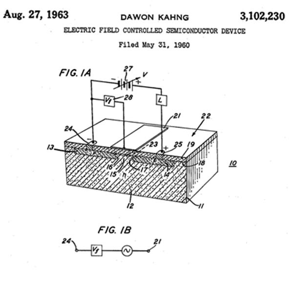
Figure showing ann Embodiment of U.S Patent No.3102230
1963: Invention of (100)-plane MOSFET and bias-temperature (BT) treatment technique (Hitachi, Ltd.)
Minoru Ohno of Hitachi and others invented the BT treatment technique, which reduces the effect of mobile ions in oxide films on the MOSFET characteristics. Through this research, they proved that using the silicon (100) plane as the channel is most advantageous for the MOSFET because it minimizes the effects of fixed charge at the interface and of the interface state between the silicon substrate and oxide film. Since then, the silicon (100) plane has been used for most LSI circuits.
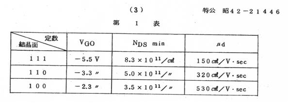
Characteristics Comparison of MOSFET with different crystal orientation
1963: Invention of CMOS (Fairchild Semiconductor)
F. M. Wanlass of Fairchild presented the basic concept of complementary MOS (CMOS) at the 1963 IEEE ISSCC, and predicted that CMOS would be advantageous for high-density integration because of its low consumption of power-on standby.
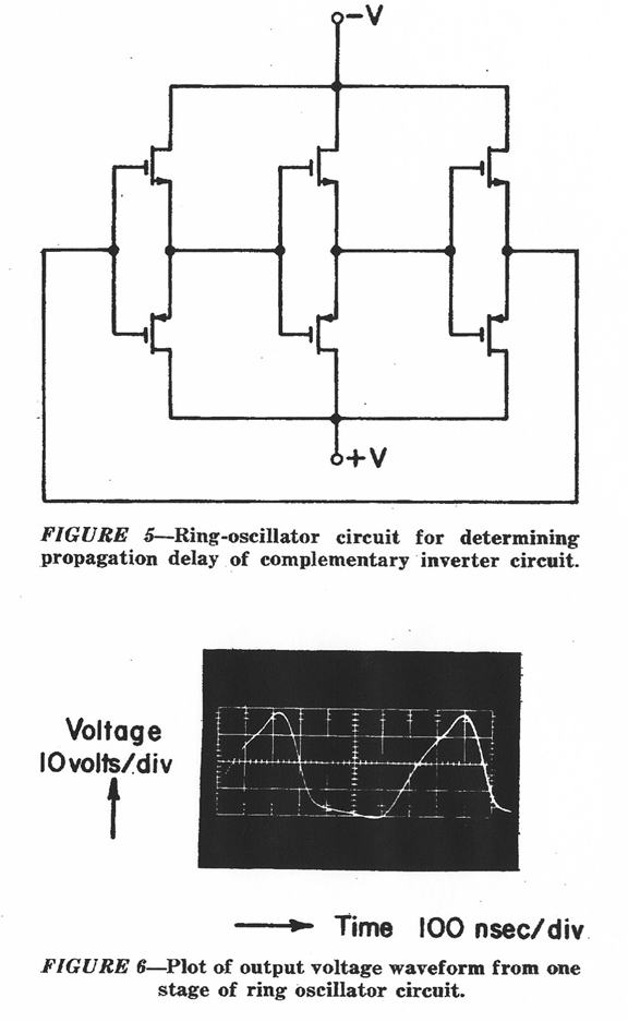
Circuit of and Waveform from World’s First CMOS Ring Oscillator
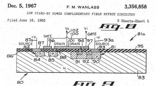
P-Well CMOS Structure in Specification for U.S. Patent No. 3356858
April 1968: Invention of mesh-emitter transistors for the UHF band (Fujitsu Limited)
An effective way to increase the output power from a bipolar transistor in high-frequency operation is to lengthen the emitter boundary per unit area, so a transistor where the emitter diffusion layer was arranged in a mesh pattern was devised. A transistor with 10 W of output power in the UHF band was developed and used in all-solid-state TV satellite equipment.
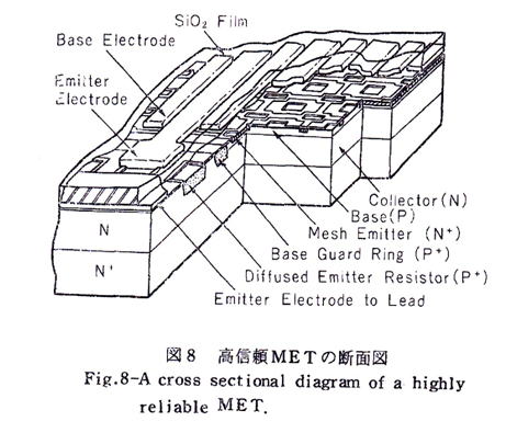
Schematic Cross-Sectional View of Mesh-Emitter Transistor
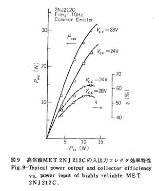
Input-Output Characteristics of Mesh-Emitter Transistor
September 1969: Invention of the DSA MOSFET (Electrotechnical Laboratory)
The DSA (diffusion self-aligned) MOSFET is formed by double-diffusing p-type and n-type impurities through a diffusion window on an n-type silicon substrate surface to create an npn structure. A region in the p-layer near the surface of the substrate is used as the MOSFET channel. As the impurity diffusion process determines the channel length, a shorter channel can be obtained than with lithography. Along with the expected usage as a short-channel MOSFET, the DSA MOSFET was also developed as a power MOSFET because of its high breakdown voltage.
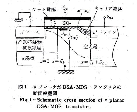
Schematic cross section of πplanar DSA-MOS transistor